
Nanoscale optics, imprinted at the scale of a production line
Our roll-to-plate platforms replicate features below 100 nm across square-metre glass and polymer panels, consistently and at high throughput.
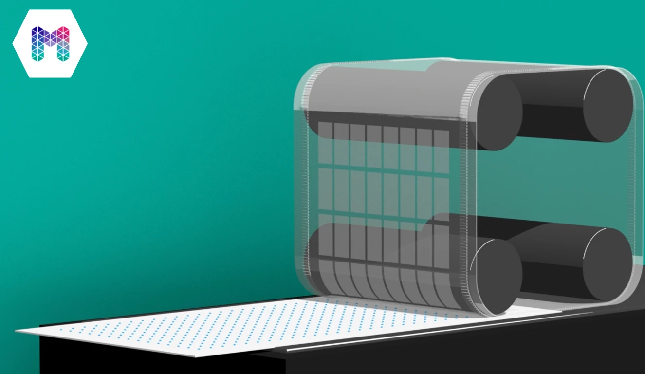
Explore the platforms- CoatA slot-die bar lays a thin film of UV-curable resin across the glass.
- ImprintThe roller presses a flexible stamp into the resin, so the nanostructure is copied line by line.
- CureUV light fixes the structure while the stamp is still in contact.
- ReleaseThe stamp peels away and the panel leaves with a permanent optical layer.
0.00 m² of a 1.30 m² panel imprinted
Wafer-level precision on panels far beyond wafer size
Hardware, process know-how and proprietary materials come from one team in Veldhoven, so the structure you design in the lab is the structure you ship in volume.
Precision you can measure
- Sub-100 nm features across m² surfaces
- Single-digit micron alignment on Cypris
- High pattern fidelity panel to panel
Throughput you can plan on
- Cycle times under two minutes on Aurora
- Rigid and flexible substrates
- Proven 24/7 commercial operation
Where our imprints end up
From the waveguide in a pair of AI glasses to the 3D layer on a large display, the same roll-to-plate principle scales to each product.
AR and AI glasses
Waveguide gratings for smart glasses, from wafer pilot runs to multi-wafer volume production.
Advanced screens
Microtextures for naked-eye 3D and anti-glare layers on panels up to 1.3 m².
Lenticular lenses
Lenticular lens arrays for 3D displays, replicated across the full panel.
Smart glass
Imprinted spacers that make smart glass more affordable, developed with eLstar Dynamics.
Photonic components
Micro- and nano-optical structures for advanced photonic components.
Etch masks
Imprinted resist patterns that serve as precise masks for downstream etching.
Our nanoimprint specialists answer technical questions directly.
One platform family, from first sample to volume
Every system shares the same imprint principle, so a process qualified in our Competence Center transfers to your fab.
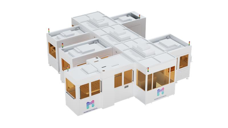
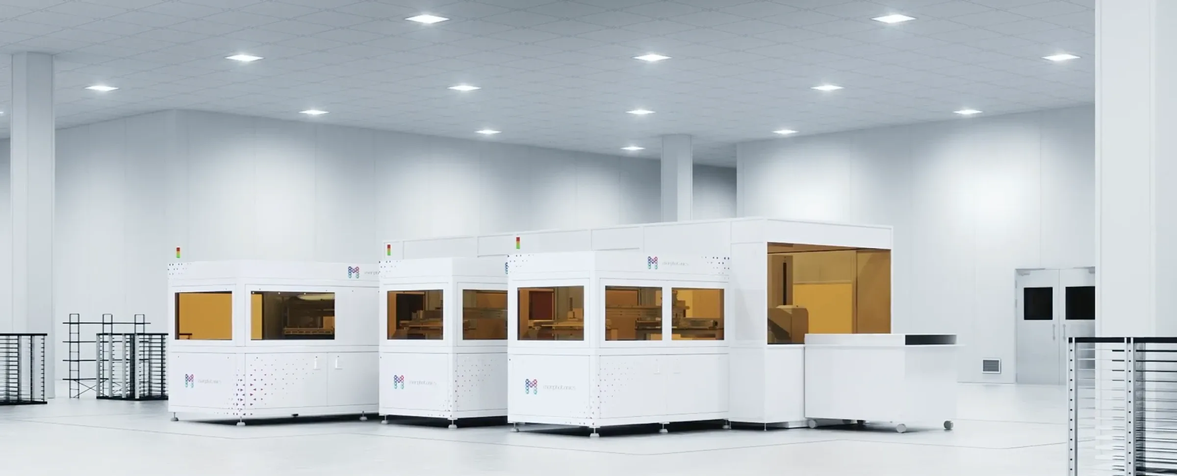
A fully automated, modular line for smart-glasses waveguides. Nanoimprint lithography and high-resolution inkjet printing run side by side, fed by robotic handling.
- XNIL imprint module with single-digit micron alignment
- Multiple-wafer handling with carriers
- Built for the move from pilot line to volume
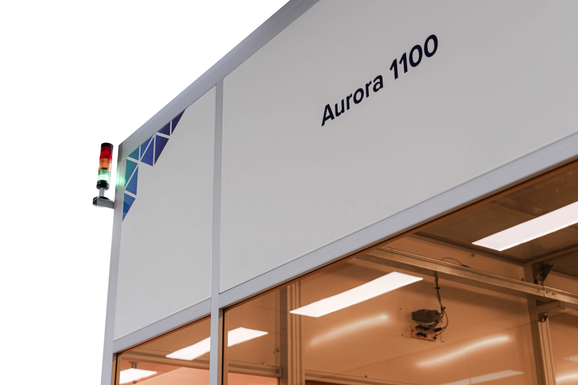
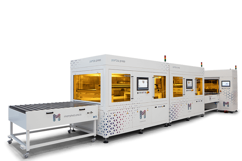
Continuous mass production of advanced screen layers. Primer, coater and imprint modules are integrated in one automated flow with proven 24/7 commercial performance.
- Sub-40 nm accuracy on panels up to 1.3 m²
- Cycle times under two minutes, TAKT of 90 s possible
- CES 2022 Innovation Award honoree
Standalone Coater (C1100), Imprint (NIL600 and NIL1100) and Primer (P1100) units that you configure and extend as your production requirements change.
- Configurable and expandable
- Compatible with your pre-treatment and post-processing
- Market-agnostic modular system
Our software suite monitors every run in real time, and our process-critical resins and flexible stamps are engineered for the platforms they run on.
- Data-driven quality control and predictive maintenance
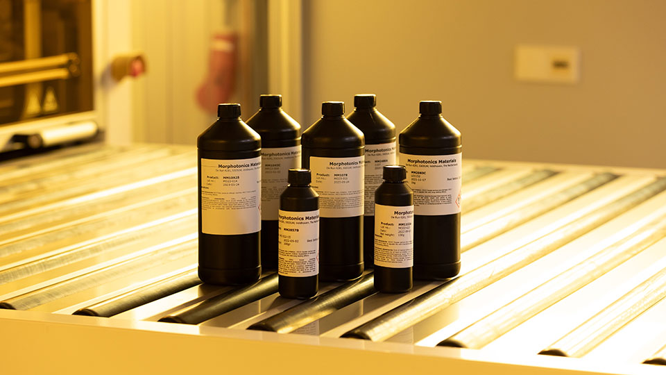
- Proprietary resins and flexible stamps
- Process alignment from day one
Roll-to-roll volume with the fidelity of wafer imprinting
We combine the throughput of roll-to-roll production with the replication quality of wafer-scale UV nanoimprint lithography. Wafer NIL is accurate but small and slow, photolithography is large but limits pattern choice. Roll-to-plate keeps the strengths of both.
Wafer UV-NIL
High position accuracy, but small substrates, low throughput and a high cost per part.
Large-area nanoimprinting
High accuracy and pattern freedom on small and large substrates, at high throughput and a low cost per part.
Large-area photolithography
Large substrates, with a limited choice of patterns.
Partners who scaled with us
“Leia Inc. has successfully industrialized the Leia proprietary Diffractive Light field Backlighting (DLB™) technology for naked eye 3D with the support of the deep knowledge Morphotonics has in large-area nanoimprint lithography processing and tool manufacturing.”
“We have a great development partner in Morphotonics and we have together successfully created joint AR demonstrators with masters from NILT and replication at Morphotonics.”
“Using NIL to create spacers is a new innovative process that enables flexibility in the spacer process, making smart glass sustainable and even more affordable.”
“CSEM is extremely glad to have found in Morphotonics a competent and highly dedicated partner in roll-to-plate (R2P) UV imprint on large area substrates.”
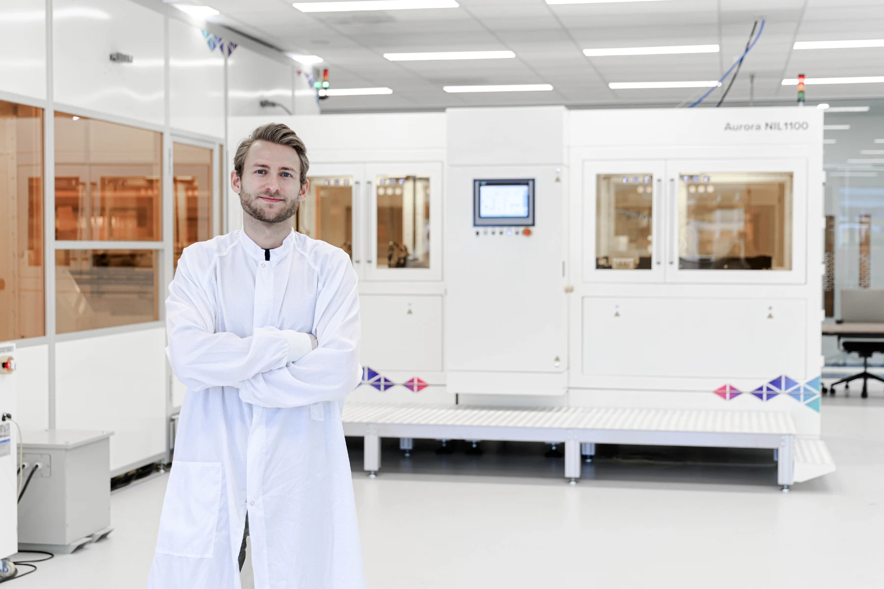
Bring your design to our cleanroom
Two ways to start, depending on where you are.
Device and component makers
Test your master in our 1,000 m² Competence Center and get process data before you commit to equipment.
Book a process trialResearch and supply partners
Join the lab-to-fab network of mastering, materials and metrology partners around our platforms.
Contact partnerships